Home » Without Label » Fermi Level In Semiconductor - Fermi Level Of Intrinsic And Extrinsic Semiconductors Physical Electronics Youtube : T is the absolute temperature.
Fermi Level In Semiconductor - Fermi Level Of Intrinsic And Extrinsic Semiconductors Physical Electronics Youtube : T is the absolute temperature.
Fermi Level In Semiconductor - Fermi Level Of Intrinsic And Extrinsic Semiconductors Physical Electronics Youtube : T is the absolute temperature.. Fermi level is a kind of measure of equilibrium electronic energy of a solid material. The fermi level lies between the valence band and conduction band because at absolute zero temperature the electrons are all in the lowest energy state. If you can bring the fermi level high enough, then part of the tail will go over to the conduction band. The electrical conductivity of the semiconductor depends upon the total no of electrons moved to the conduction band from the valence band. However as the temperature increases free electrons and holes gets generated.
Kb is the boltzmann constant. 1.1 0, indicating equal concentrations of electrons and holes. Of electrons in conduction band are greater than no. At absolute zero temperature intrinsic semiconductor acts as perfect insulator. This probability of occupation of energy levels is represented in terms of fermi level.
Fermi Level In Extrinsic Semiconductor from www.physics-and-radio-electronics.com In a perfect semiconductor (in the absence of impurities/dopants), the fermi level lies close to the middle of the band gap 1. The fermi level plays an important role in the band theory of solids. The fermi level is the surface of fermi sea at absolute zero where no electrons will have enough energy to rise above the surface. 1.1 0, indicating equal concentrations of electrons and holes. 1.1 0, indicating equal concentrations of electrons and holes. The electrical conductivity of the semiconductor depends upon the total no of electrons moved to the conduction band from the valence band. This definition of fermi energy is valid only for the system in which electrons are free (metals or superconductor), or any system. If you can bring the fermi level high enough, then part of the tail will go over to the conduction band.
Kb is the boltzmann constant.
Kb is the boltzmann constant. Due to lack of sufficient energy at 0 kelvin, the fermi level can be considered as the sea of fermions (or electrons) above which no electrons exist. The fermi level is referred to as the electron chemical potential in other contexts. Ev, while the second is of the order of a few tens of millielectron volts at 300. Fermi level is the state for which there is a 50% probability of occupation. Of holes in valance band. K.consequently, we see from this equation that the fermi level should typically lie very close to the middle of the energy gap in intrinsic semiconductors. We show that this problem can be overcome by using 2d. The fermi level represents the electron population at energy levels and consequently the conductivity of materials. However as the temperature increases free electrons and holes gets generated. • all energy level in one band is same energy. To a large extent, these parameters are key ingredients that define. Kb is the boltzmann constant.
To a large extent, these parameters are key ingredients that define. Of free electrons in conduction band. Whenever the system is at the fermi level, the population n is equal to 1/2. Ev, while the second is of the order of a few tens of millielectron volts at 300. However as the temperature increases free electrons and holes gets generated.
Gate Ese Detailed Explanation Of Fermi Level In Intrinsic Semiconductor In Hindi Offered By Unacademy from edge.uacdn.net Ec is the conduction band. We show that this problem can be overcome by using 2d. The correction term is small at room temperature since eg ~ 1 ev while kbt ~ 0.025 ev. Green, unsw) illustrating the location of the fermi level e f relative to the valence and conduction bands for various materials. T is the absolute temperature. Semiconductor doping and higher temperatures can greatly improve the conductivity of the pure semiconductor material. The fermi level is referred to as the electron chemical potential in other contexts. At absolute zero temperature intrinsic semiconductor acts as perfect insulator.
For the intrinsic semiconductor at 0k, is fermi energy and fermi level both are equal?
Of holes in valance band. • all energy level in one band is same energy. Fermi level is the state for which there is a 50% probability of occupation. (18) is of the order of 1. Kb is the boltzmann constant. If you can bring the fermi level high enough, then part of the tail will go over to the conduction band. Fermi level is a kind of measure of equilibrium electronic energy of a solid material. Fermi level of extrinsic semiconductor extrinsic semiconductors are formed by adding suitable impurities to the intrinsic semiconductor. Position of fermi level in intrinsic semiconductors • width of conduction band and valence band is small as compared to forbidden energy gap. Fermi level of intrinsic semiconductor those semi conductors in which impurities are not present are known as intrinsic semiconductors. Above is a diagram (ref. This probability of occupation of energy levels is represented in terms of fermi level. Of electrons in conduction band are greater than no.
K.consequently, we see from this equation that the fermi level should typically lie very close to the middle of the energy gap in intrinsic semiconductors. Semiconductor doping and higher temperatures can greatly improve the conductivity of the pure semiconductor material. T is the absolute temperature. Ec is the conduction band. There are bands crossing the fermi level, so the material is metallic.
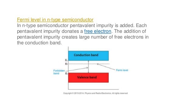
Fermi Level In Extrinsic Semiconductor from image.slidesharecdn.com The fermi level is the surface of fermi sea at absolute zero where no electrons will have enough energy to rise above the surface. However as the temperature increases free electrons and holes gets generated. The fermi level is the energy separating occupied states of the valence band from empty states of the conduction band at the absolute temperature t=0 kelvin. Due to lack of sufficient energy at 0 kelvin, the fermi level can be considered as the sea of fermions (or electrons) above which no electrons exist. The added impurity is very small, of the order of one atom. Of electrons in conduction band are greater than no. This probability of occupation of energy levels is represented in terms of fermi level. Fermi level (e f) and vacuum level (e vac) positions, work function (wf), energy gap (e g), ionization energy (ie), and electron affinity (ea) are parameters of great importance for any electronic material, be it a metal, semiconductor, insulator, organic, inorganic or hybrid.
• all energy level in one band is same energy.
Due to lack of sufficient energy at 0 kelvin, the fermi level can be considered as the sea of fermions (or electrons) above which no electrons exist. Ec is the conduction band. This definition of fermi energy is valid only for the system in which electrons are free (metals or superconductor), or any system. The electrical conductivity of the semiconductor depends upon the total no of electrons moved to the conduction band from the valence band. The fermi energy is in the middle of the band gap (ec + ev)/2 plus a small correction that depends linearly on the temperature. Ec is the conduction band. The fermi level represents the electron population at energy levels and consequently the conductivity of materials. Of holes in valance band. The fermi level pinning effect is strong in many commercially important semiconductors (si, ge, gaas), and thus can be problematic for the design of semiconductor devices. T is the absolute temperature. Kb is the boltzmann constant. Green, unsw) illustrating the location of the fermi level e f relative to the valence and conduction bands for various materials. The term fermi level is mainly used in discussing the solid state physics of electrons in semiconductors, and a precise usage of this term is necessary to describe band diagrams in devices comprising different materials with different levels of doping.